In terms of ultraviolet LED technology
In the first quarter, UV industry chain enterprises strengthened their research and development of UVC LED technology. 256nm Japan created a UVC LED with a luminous efficiency of 50mW through its exclusive AIN UV LED technology, and continued to strengthen its technology to develop 200MW products. The 275nm deep ultraviolet LED has achieved a luminous efficiency of 20mW at 100mA and has achieved stable mass production and shipment; The luminous efficiency of 280nm deep ultraviolet LED is 55mW at a current of 350mA; The luminous efficiency of 230nm deep ultraviolet LED is 1.6mW at a current of 100mA. In addition, Asahi Chemical has collaborated with Nagoya University to develop a laser diode that emits deep ultraviolet light, using a specially designed p-side layer to achieve sufficient light confinement and reduce device resistance, as well as to suppress light scattering loss by using an AIN substrate with fewer defects.
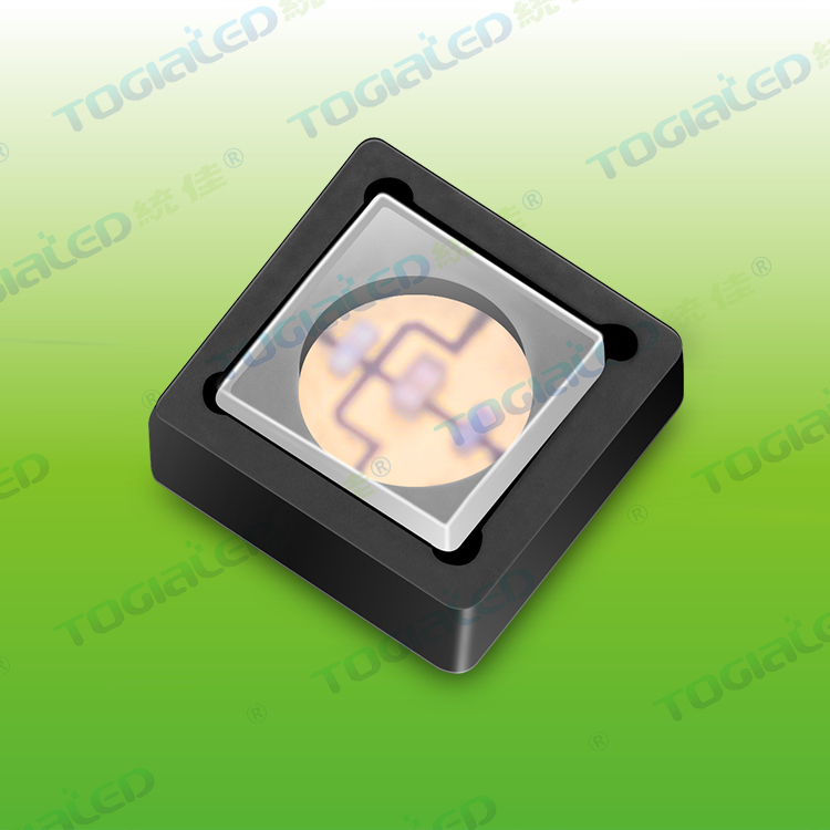
In terms of ultraviolet LED products
The outbreak of the epidemic has stimulated the market for sterilization and disinfection products. Domestic and foreign manufacturers have launched various UV LED products to meet the needs of sterilization and epidemic prevention. In addition to UVC LED packaging and modules, there are also a variety of application end products such as UV LED sterilization robots, sterilization sweeping robots, sterilization rods, and sterilization flashlights.
UV LED production line and investment
In terms of production capacity and production lines, in the early first quarter, due to the impact of the epidemic, there was a delay in resuming work, which had a certain impact on enterprises. With the orderly progress of national resumption of work and production, LED companies from Shenzhen Foreign Exchange have reported a significant increase in order volume compared to the same period last year.
In terms of investment, industry enterprises are increasing their investment in the field of deep ultraviolet semiconductors, and domestic top tier manufacturers and segmented leading companies in the deep ultraviolet LED field are expected to benefit. The Zhongke Lu'an Phase I 30 million deep ultraviolet LED chip project has been successfully put into production, becoming the world's first mass-produced deep ultraviolet LED production line. The Zhongke Lu'an Shenzhen UV Optoelectronics Project is located in the Zhangze New Industrial Park of Changzhi High tech Zone. The project is constructed in two phases with a total investment of approximately 2 billion yuan. At present, the first phase of the 30 million chip production line project has been fully completed and accepted. It is expected to complete the construction of the second floor packaging pilot line in the workshop by the end of August 2020. At the same time, preliminary preparations for the second phase of the 300 million chip project will be carried out, and construction will begin in the second half of the year. Mulin Sen and Zhishan Semiconductor jointly enter the deep ultraviolet field, with a project valuation of 123 million yuan. Mulin Sen invested 36.9 million yuan to acquire a 30% equity stake in Shenzhen Zhishan, and is expected to fully benefit from the growth of demand in the deep ultraviolet market in the future.
Introduction of UV LED project
Nanjing, Jiangsu and Changzhi, Shanxi have successively introduced ultraviolet industry chain projects, with a disclosed project amount of 900 million yuan. At the China US Science and Technology Center Investment Promotion Conference in Nanjing Pukou Economic Development Zone, a semiconductor material, chip, and related technology application project with a total investment of 200 million yuan will be committed to solving the technical difficulties of deep ultraviolet chips. This project will have huge market prospects in areas such as water purification, air, white goods, and daily fast-moving consumer goods, and will be widely used in radar and detection fields. Shanxi Changzhi National High tech Development Zone has introduced third-generation semiconductor UV packaging, GaN epitaxy, chip and application research and development promotion projects. The project signing companies are Shanxi Huawei UV Semiconductor Technology Co., Ltd. and Shanxi Zhongweixin Semiconductor Technology Co., Ltd., with a total investment of 700 million yuan. The main focus is on third-generation semiconductor UV device packaging and application, GaN epitaxy, chip production and manufacturing, and power device packaging, including UVC devices, UV sensors, UV detectors, power semiconductors, etc., which are widely used in home appliance disinfection, communication, and national defense.